Part I: Morris Chang's 2021 Speech on the History and Future of Semiconductors
"TSMC's business model is that semiconductor companies are our customers, our friends."
Today’s post is the translation of an hour-long speech Morris Chang delivered on the history and future of semiconductors and TSMC in April 2021 in Taiwan. (The original video of the speech, delivered in Chinese, can be found here.) Due to the length of the speech, we are publishing it in two parts. Today’s post is Part I. This translation also includes screenshots of the slides (in traditional Chinese) Chang used during his speech.
Given the semiconductor industry’s increasing geopolitical importance and TSMC’s “friendshoring” to America, this speech is especially worth reading, as it is an unfiltered and honest view from one of the remaining “founding fathers” of the semiconductor technology — Morris Chang — including his perspetive on whether Arizona is a wise choice to build TSMC’s next fabs. I hope you enjoy reading it and pondering about it.
First of all, thank you very much, President Huang and Editor-in-Chief Fei of the Economic Daily News, for giving me this opportunity to speak on a topic that I have felt is very important in the past year or two. I would also like to thank all the distinguished guests who have come to speak here, Chairman Mark Liu and President CC Wei of TSMC, all the distinguished guests who have come to listen, and friends from the media.
Ladies and gentlemen, the title of my speech today is "Cherishing the Advantages of Taiwan's Semiconductor Wafer Manufacturing", and this speech is an appeal from me to the Taiwanese government, Taiwanese society, and TSMC.
My status is a TSMC retiree, and I no longer have any authority inside the company, which is my choosing, so TSMC is also a very important audience of what I’m advocating for in my speech today.
Because I already know that the vast majority of the audience is not in the tech community, much less the semiconductor community. So I would like to talk a little bit about the history of semiconductors, otherwise jumping straight into the key point —— the advantages of Taiwan's semiconductor wafer manufacturing —— might be too confusing.
This is the PowerPoint I made today. The first chapter starts with a brief history of semiconductors; the second chapter talks about the importance of semiconductors and why they have become a must-have for politicians and geopolitics. Then I will talk about the division of labor in the semiconductor industry. If it were not for this division of labor, we would not have the problems we have today. This division of labor started decades ago.
The fourth chapter will be the main topic - Taiwan's advantages in wafer manufacturing; the fifth one will be the fab-centered semiconductor industry chain, because the impact of wafer manufacturing on Taiwan is definitely not only on TSMC. TSMC’s wafer manufacturing has also driven a lot of other upstream, downstream and midstream industries.
Sixth, I’ll talk about the founding of the professional wafer manufacturing industry, that is, the founding of TSMC. This took people, opportunities, and a bit of luck or coincidence to happen (风云际会). It’s very rare so I think it’s hard to produce even one example from an entire generation. Seventh, TSMC's success; eighth, TSMC's status today; in the ninth, tenth, and eleventh chapters, I want to look at our foreign competitors, the United States, mainland China, and South Korea. These three are the most important competitors, although, of course, there are also Japan, Europe. However, because my topic today is wafer manufacturing, comparatively speaking, the United States, mainland China, and South Korea are our important competitors.
Finally, the twelfth point, since now people often say, "ah, we can have another so-called 'protective mountain of the nation'” (护国神山, i.e. an industry or company as influential to Taiwan as TSMC), I also want to talk about the possibility of producing the next "protective mountain of the nation." And lastly, the conclusion.
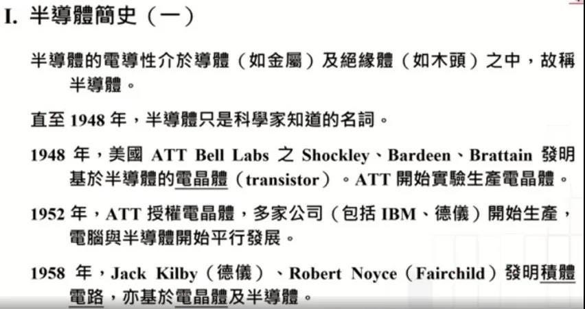
A Brief History of Semiconductors
The conductivity of a semiconductor is between that of a conductor (metal) and an insulator (wood). You can control the conductivity of the semiconductor. In short it is between metal and wood, so we call it semiconductor.
But honestly, until 1948, semiconductor was a term only known to scientists. Ordinary people, those who majored in liberal arts, business, or law didn’t know what it was. Only scientists, especially physicists, knew. So it was a very small group in society back then.
In 1948, a major event in the semiconductor industry took place. AT&T, at that time the largest telecommunications company in the United States, had Bell Labs under it, which was a world class research institution for many decades. There were three physicists at Bell Labs. Shockley was their leader, and Bardeen and Brattain didn't really like him, but the three of them collaborated to invent the transistors, which were based on semiconductors. What they invented was very important, and that was the transistor.
What is important is that it (semiconductor transistor) is very small. Prior to its invention, vacuum tubes could be used to make transistors, but vacuum tubes are big. During the Second World War when the United States began to manufacture computers, a computer was so large in size, because of the use of vacuum tubes, that it could occupy an entire room.
I came to the United States in 1949, and didn't see any computers the first year I was there. I was at Harvard, and the place where the computers were was far away from my freshman dormitory, so I didn't go. The next year, in 1950, I went to MIT, saw a computer, and learned to code. The computer was full of vacuum tubes, occupying the whole room. Honestly, the functionality of a computer as big as a room was not as powerful as the cell phone you are carrying today.
But anyway, the transistor was invented in 1948, and AT&T knew how important it was. These three physicists —— Shockley and Bardeen were theoretical physicists and Brattain was an applied physicist —— won the Nobel Physics Prize for transistors in 1956, pretty soon after the invention. Bardeen went on to win a second Nobel Prize, but that's not relevant to our topic today.
Shockley was born in the same year as my mother, and I was his student at Stanford University, where I listened to his lectures. He was a good lecturer, but the most memorable thing was his arrogance. Many students, including me, were afraid to ask him questions because when we saw other students asking him questions, the first thing he did was not to answer the question, but to taunt the student, looking down on him for asking a simple question and saying that his question was really ridiculous. In such a situation, few students dared to ask him questions and just listened to his lectures.
In 1952, AT&T knew that one company could not monopolize the transistor because it was too important for the future, so it licensed the technology to many companies, including IBM and Texas Instruments (TI). Many companies began to produce it, dozens of companies, including such large companies as GE. IBM was already quite big, but GE and RCA were even bigger than IBM. At that time, TI was a very small company, but it was also a licensee. It would become the most successful one in later decades to come.
After that, computers and semiconductors began to develop in parallel, because computers needed semiconductors the most.
I joined the semiconductor industry in 1955 after receiving my Master's degree from MIT. The history of semiconductors was irrelevant to me until 1955, and after 1955 the history of semiconductors merged with my life story.
In 1958, I had just arrived at TI. A new colleague of mine, who, like me, had just joined TI, was Jack Kilby. He was eight years older than me, but we were contemporaries. He was working on integrated circuits, which the chairman of TI asked him to do.
Jack Kilby was a very innovative person. His education level was not high —— only Master’s and no PhD. If you talked to him about theoretical physics, he wouldn’t understand it, but he was innovative. He insisted that he was an engineer, and whenever someone said he was a scientist, he would immediately deny it and say, "I am an engineer". He later invented the integrated circuit, which happened under my eyes.
That same year, Bob Noyce (or Robert Noyce) was at Fairchild, and I had just met Bob Noyce at that time. We were together at the Washington IEDM, a technical conference held in Washington every December. Noyce and Gordon Moore, who I will talk about later, were at Fairchild. I had already joined TI at that time, and I had just joined. We were quite gentlemanly at the conference together, and not aggressive with each other yet.
After the meeting, Noyce, Moore, and I went out for a beer in the evening, and at that time I was only 27, Noyce was only 31, and Moore was only 29. We were all young and excited, and thought we were the “Favored Children of Heaven” (天之骄子, i.e. children of destiny), lucky to have joined the promising field of semiconductors. After drinks and dinner, we sang our way back to the hotel from the restaurant amidst the snow drifts.
Both of them, Kilby and Noyce, invented the integrated circuit almost at the same time. In fact, Kilby was a little earlier, about a month or two earlier. But honestly, although Kilby's was a little earlier, Noyce's was a planar construction while Kilby's was a bonded construction. Without Noyce's planar construction, integrated circuits would not have been made.
Later, after some legal disputes in the court or something, both sides —— TI and Fairchild —— settled, saying that the two people jointly invented the integrated circuit. Noyce unfortunately passed away very early, in 1990, at the age of 63. He lived a full life: had a lot of girlfriends, often flew his own plane, went diving and swimming, and played many other sports.
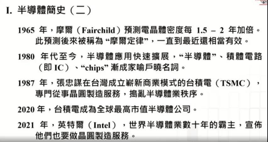
I think the next important thing (in semiconductor history) was Moore’s Law in 1965. Moore, at Fairchild, predicted that circuit density would double every 1.5 - 2 years, a prediction that came to be known as "Moore's Law" and remained quite valid until recently.
It’s been decades. Although Moore's Law is only a prediction, it has forced every company to double the circuit density every year and a half to two years, because by then the semiconductor industry was no longer gentlemanly —— companies already became aggressively competitive —— and everyone thought, “If I don’t double it, my competitors will.” So they tried their very best to do so. This was the important thing about Moore's Law. It was at first only a prediction, which might not have been true. In fact, if MOS (metal–oxide–semiconductor) was not invented, or I should say made practical, since it had existed, Moore's Law would not have been accurate. That was after Moore's Law was published, in around 1968, 1969.
Almost ten years ago, IEDM —— the same conference that I went to 50 years ago and sang my way back to the hotel —— invited me to speak on the biggest semiconductor innovations. I then put transistors and integrated circuits in the speech. I also put Moore's Law in it, because of what I just said, the pressure (to double the circuit density every 1.5 - 2 years). I also put MOS in it. MOS allows us to (let the circuit density) double, double, and double again. Lastly, I included chip foundry in the speech —— it was also listed as one of the important innovations in the history of the semiconductor industry.
From the 1980s to the present, semiconductor applications expanded rapidly, mainly PCs, and later, of course, cell phones etc. Why do I talk about the year of 1980? Because 1980 was when IBM released its PC, which universalized PCs. IBM was a big company at that time, so when people saw that IBM released a PC, they saw the PC as a legitimate thing, not just a toy. Before IBM, Apple and several small companies already came out with PCs, but people said, “hey, this might just be a toy.” IBM’s PC release in 1980 changed this notion.
Especially in the 90s. In the 80s, IBM came out and PCs became prevalent in the office, but in the 90s they became prevalent at home. Even housewives used them. I personally experienced this history and so had a deep impression of it. The 90s was also Andy Grove's era. Everyone always thinks that he is Intel's best, greatest CEO ever. This is really a case of, “Our times shape our heroes. Our heroes shape our times” (时势造英雄,英雄造时势). The 90s was the era of very rapid PC adoption, and Intel was almost exclusive in making processors, so the situation made Andy Grove a hero.
In 1987, Morris Chang established TSMC in Taiwan with a new business model, specializing in wafer manufacturing services. This was a disruptive innovation that disrupted the semiconductor industry, and I'll explain why in a moment. In 2020, TSMC became the world's largest semiconductor company by market capitalization.
Intel was the dominant player in the world's semiconductor industry for decades, from the late 1980s until recently. TI's period of dominance was from the 60s to mid-80s. Last year, TSMC reached its highest market cap at $600 billion, when Intel had just over $200 billion, less than half of TSMC. However, what will happen after this is not certain.
In 2021, Intel, the former dominant player, announced that they are also going to provide wafer manufacturing services. This is quite ironic to me. Originally they were the dominant player, and frankly they looked down on wafer manufacturing, thinking that this thing couldn't do much. I was acquainted with them, so at first I sought investment from Intel. At that time, in 1985, TSMC was raising capital, but the timing was not right and the economy was not good, so Intel refused to invest.
However, after TSMC was established, Intel, Andy Grove, and Gordon Moore helped a lot, but they never thought that this foundry business model would become so important; nor did they ever think that one day they would also do wafer manufacturing. Of course, Gordon Moore is now in very bad health and lives on Big Island, Hawaii. Noyce, as I just said, has died, and Andy Grove has also passed away.
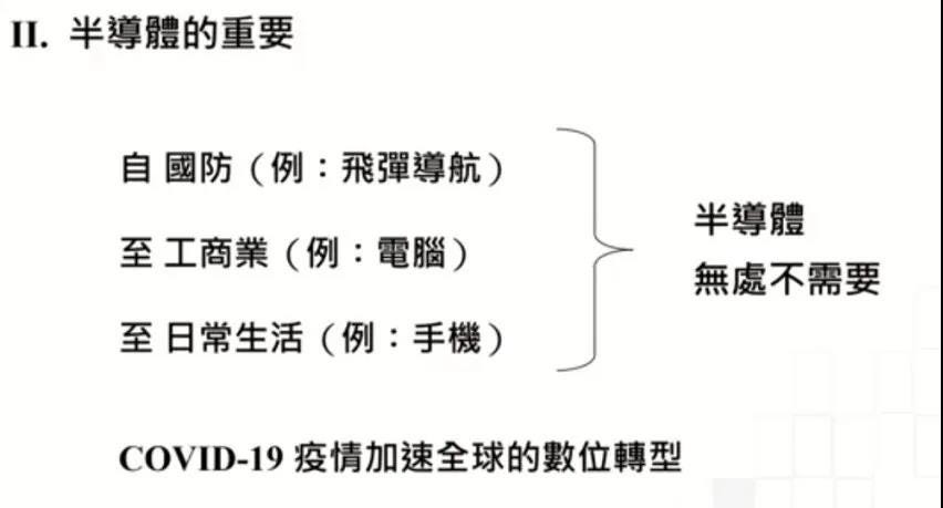
Importance of Semiconductors
I’ve talked about history for a long time, so now we can go a little faster. The importance of semiconductors can be first of all seen in national defense: missile navigation, GPS, this is another small story.
Now we are very familiar with GPS because all the cars have it. The first time I heard about GPS was at TI. I had top-secret clearance at TI, and was in charge of semiconductors. TI had a defence system division and they needed integrated circuits to do GPS to navigate the missile. I heard them talk about it and thought that it was super cool, “how can it hit within 5 ft diameter of a target from thousands of miles away?” This was in the 70s. Now every car has GPS.
Semiconductors are ubiquitous now, in commerce, industry, and daily life, from computers to cell phones. And of course, Covid19 has accelerated the global digital transformation.
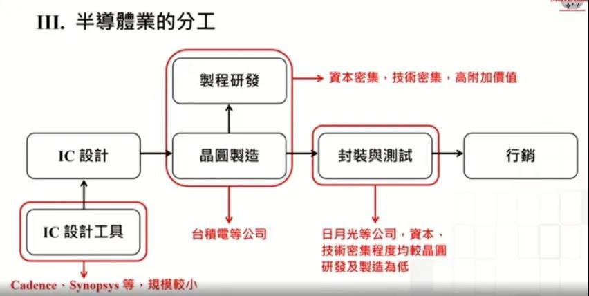
Division of Labor in the Semiconductor Industry
Originally, when I first joined the semiconductor field in 1955, there was no division of labor in the industry. Every company did everything by themselves. They did IC design —— sorry, there was no IC in 1955. It was transistors, but a few years later there would be IC. IC design needed design tools, but each company would do it on their own. Design is actually quite technology-intensive, the added value is also quite high, but it’s not so capital-intensive, so it doesn’t require a lot of capital. Process R&D and wafer manufacturing are capital-intensive, technology-intensive, and have high added value. The technology and capital required for packaging & testing are not as intensive as that for wafer manufacturing. Compared to IC design, packaging & testing is more capital-intensive but not as technology-intensive. In short, every semiconductor company did its own thing.
The division of labor can be said to have begun in the 1960s and the first to have been separated out was packaging & testing. Companies often still did it themselves, but in low-wage areas, such as Taiwan, the Philippines, Singapore, Hong Kong (Hong Kong was where they started), and even Japan. In the 60s, you know that Japan's wages were only 5% of that in the United States. At that time, I suggested that TI come to Taiwan, and the CEO of TI said, "Let's go to Japan, because the salary in Japan is only 5%. In Taiwan it’s only 1%, but the difference between 1% and 5% is not big.” However, I told him at that time that Japan's wages would rise quickly, while Taiwan's wages would not rise so fast, so he came to Taiwan. This is just a small anecdote.
In short, packaging & testing in the 60s was at first not technically separated out, but done by individual companies in low-wage regions. However, in low-wage areas, you couldn’t lock up the market and have it all to yourself. Low-wage areas also had entrepreneurs. And regardless of whether you were TI or Motorola, they saw that you engaged in packaging & testing here. They knew that this technology was not that difficult, so they would open companies that had lower overhead than you and would say, "hey, you should let us do it for you". That’s why there are a lot of packaging facilities in Korea and so on.
It was like that in the semiconductor industry till 1985. I was in New York at General Instrument then. Gordon Campbell was a pretty famous entrepreneur who had founded a semiconductor company that was quite successful. In 1984, he had just sold it and wanted to build a new company. I didn't really know Gordon Campbell, but I knew his name, and he knew my name. He said, "I'm hoping that you and General Instrument can invest [in my new company]. Can you come and take a look?”
So we made an appointment, and he came to see me and said he needed $50 million. I said, "Do you have a business plan?" He said, "The business plan is all in my head.” Then I said, "Even if I want to invest in your company, I have to report this to General Instrument's board of directors. There must be a business plan.” He said, “No problem, no problem Morris. I'll send it to you in two weeks.”
He went back —— he was in California while I was in New York —— but 3 weeks passed and nothing happened. I was actually quite interested, so I called him. He said, "I'm sorry Morris, I didn't contact you again because I don't need 50 million anymore. I just need 5 million, 5 million is enough, and I can get that together myself. ” When I asked why, he said, “I’m not going to do wafer manufacturing —— that is capital intensive —— I will just build a design company.”
This was the first time I had heard of a company specializing only in design. Of course, the complementary part of that is wafer manufacturing: since there are companies specializing in design, there can also be companies specializing in wafer manufacturing. It took me a year to figure out this complementary model, which became TSMC. Anyway, I originally thought this speech would be too short, but it seems too long now.
Why is this business model so disruptive? Because process R&D and wafer manufacturing are in fact the heart of the so-called IDM (integrated device manufacturer). Packaging & testing can be separated out, but process R&D and wafer manufacturing are at least part of the heart, the other part being IC design.
TSMC's business model is that semiconductor companies are our customers, our friends. This is the biggest discovery of this business model. The biggest discovery of a business model is who your customer is and how you make money. Since our customers are semiconductor companies, if they originally make their own wafer but now we make wafer too, then our competitors are those in charge of wafer manufacturing inside semiconductor companies. That's why it's very disruptive. You young listeners haven't experienced this kind of corporate politics —— this is very disruptive.
Taiwan’s Advantages in Wafer Manufacturing
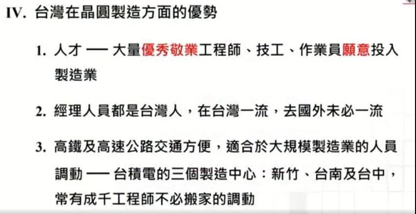
First of all, we have talent, a large number of excellent and dedicated engineers, technicians, operators willing to commit to manufacturing. This is very important. At least in the United States, engineers are not as dedicated as those in Taiwan. I think people in other professions as well, haha. Americans are not as dedicated as Taiwanese.
So what I want now are excellent and dedicated engineers, technicians, and operators, all of whom are important and need to be willing to commit to the manufacturing industry. Manufacturing in America is no longer a “hot” industry. It has not been “hot” for decades. People don’t want to work in the manufacturing industry. There are a lot of nerds doing R&D; there are a lot of people in the financial sector —— engineers etc. can also be in the financial sector and do venture capital and private equity. There are also many people doing marketing. All of the above (i.e. R&D, finance, marketing) are more desirable fields to be in than manufacturing. The commitment to manufacturing is a great advantage of Taiwan.
Secondly, our managers are Taiwanese. In Taiwan they’re the best, but they may not be the best when working overseas. So is the reverse —— my own experience demonstrates this. I worked for two or three decades in the United States to reach the level just below the CEO of a large company, but coming back here to Taiwan, even managing teams of a much smaller scale messes up my brain. Culture, habits, and language are all different. Although I had been speaking Chinese till I was 18, 36 years of not using it made it a problem for me to speak it again at the age of 54. I’m afraid it’s probably still a problem today, haha.
Another advantage Taiwan has is its convenient high-speed rail and highway transportation system, which makes mass manufacturing personnel movement easy. TSMC's three manufacturing centers —— Hsinchu, Tainan, and Taichung —— often have thousands of engineers whose location assignment changes but who do not have to move their family. They can be transferred from Tainan to Taichung, or Hsinchu to Taichung. The time from Tainan to Hsinchu is a little longer, so that’s not a one-day commute anymore, but the commute between Taichung and Tainan, and Hsinchu and Taichung, are within a day. Even when transportation is convenient, TSMC also has dormitories so that engineers can have a place to stay during the week and go home on weekends. They don’t have to move their whole family when their new assignment is often only a year. How do you do that in Arizona?
…
We will publish Part II of this speech next week.


